18860953668
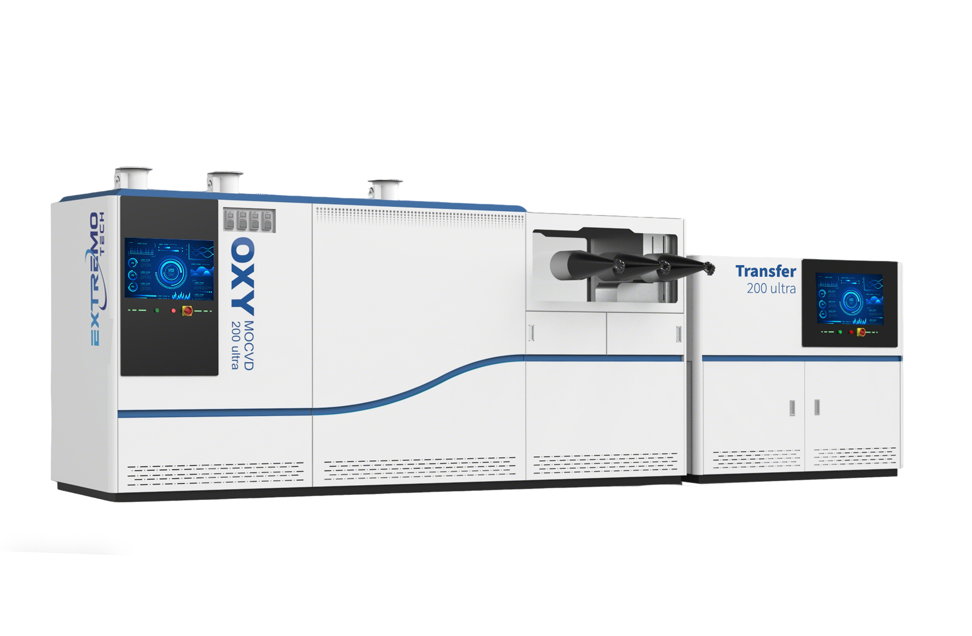
Product Introduction: This integrated system comprises two units: the 2D semiconductor single-crystal MOCVD system (Model Oxy MOCVD 200 Ultra) on the left, and the fully automatic vacuum transfer system (Model Transfer 200 Ultra) on the right.
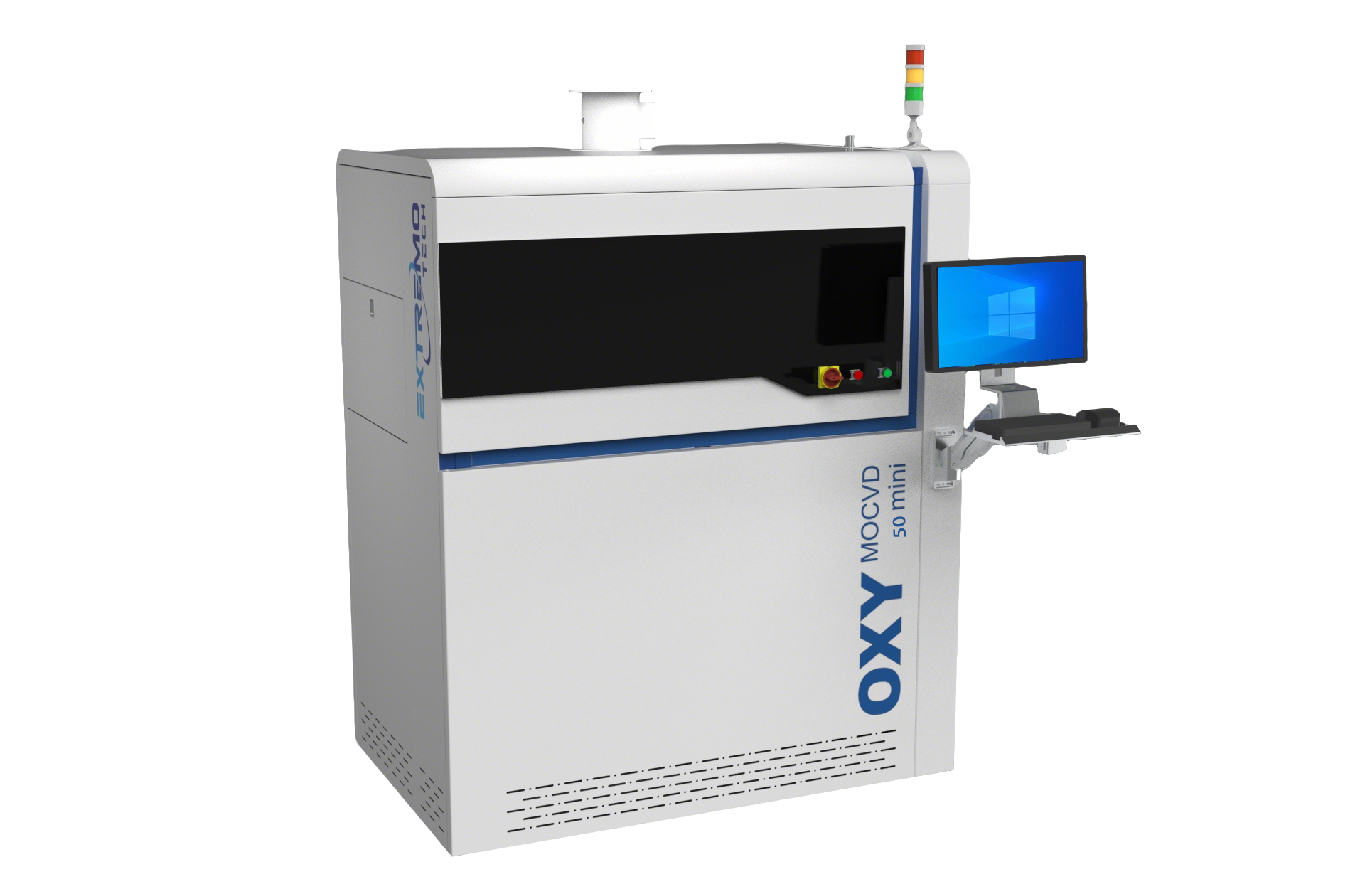
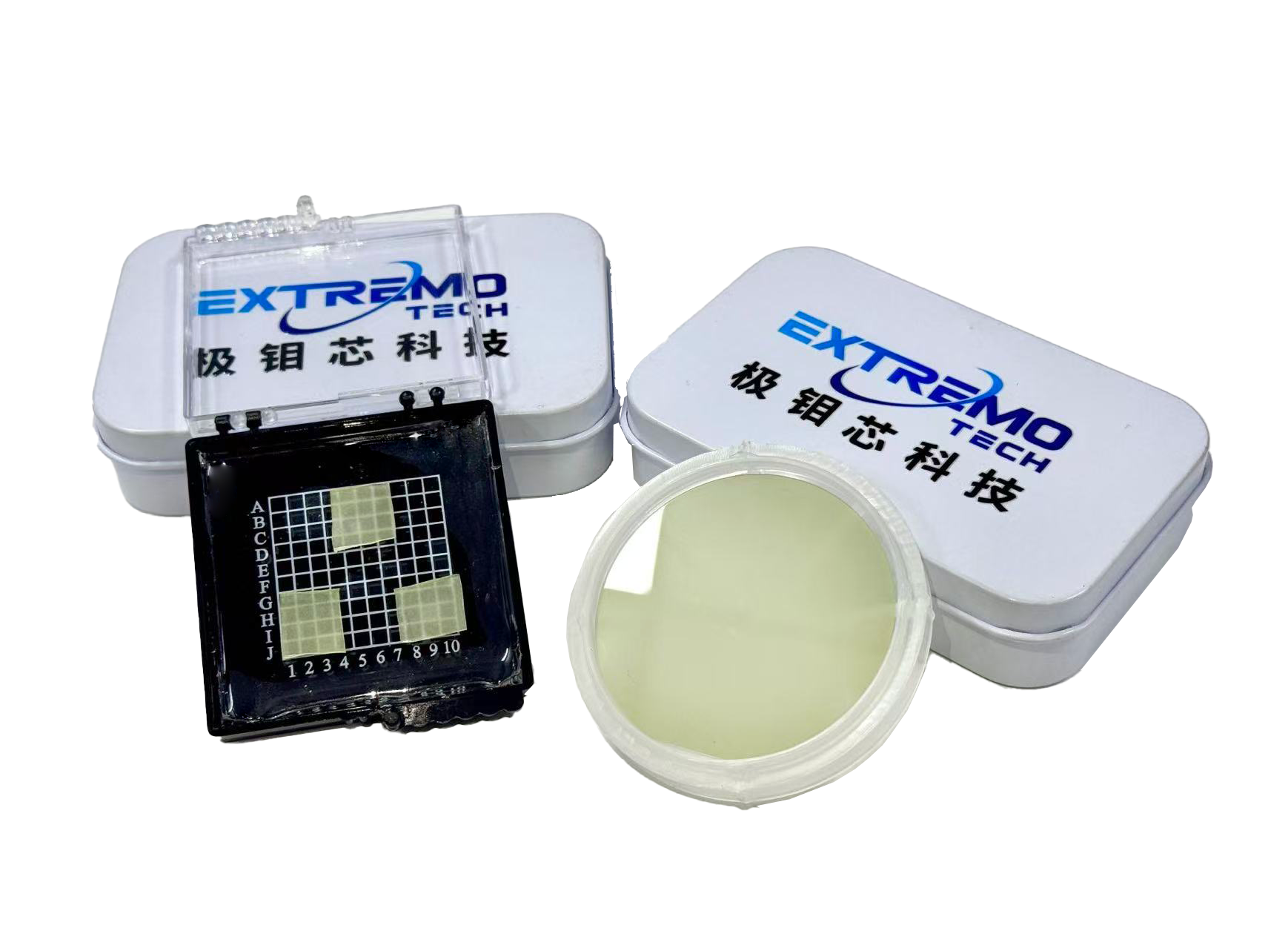
It achieves in-plane film uniformity above 99.5%, controllable layer thickness and low defect density. For 6-inch wafers, the carrier mobility at arbitrary positions exceeds 100 cm²V⁻¹s⁻¹. It outperforms traditional CVD systems in repeatability and stability, acting as the core equipment for next-generation integrated circuit fabrication.
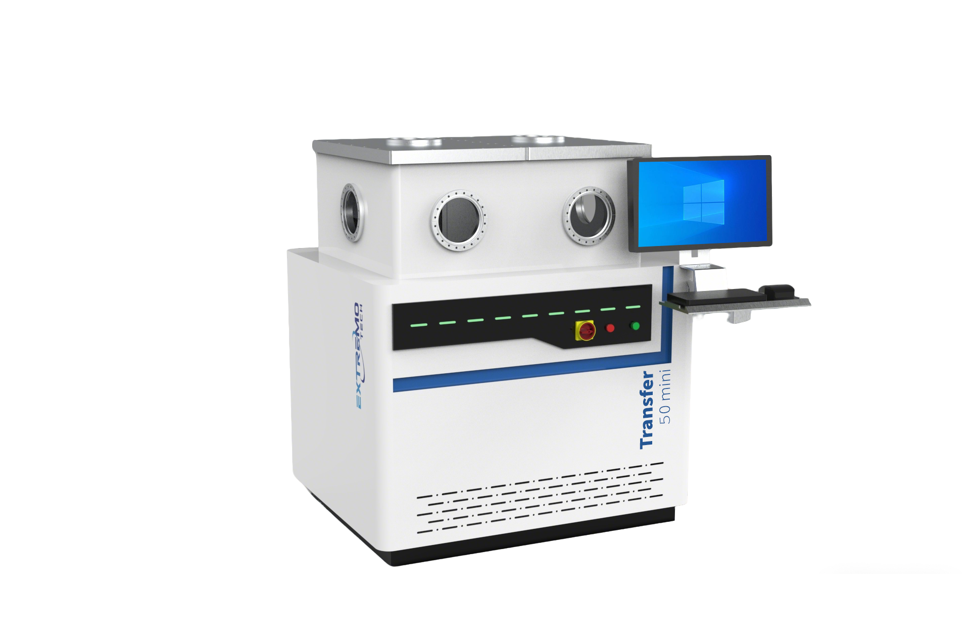
With a modular structure, it integrates ultra-high vacuum chambers for stripping, transmission and release. Equipped with a multi-DOF precision manipulator, it realizes micron-level precise positioning and damage-free transfer of wafer-level samples in a clean vacuum environment.
The whole process is completed under vacuum, effectively preventing interface contamination and structural damage. It breaks through the core technical bottleneck of 2D material transfer, and provides strategic support for the localization and leapfrog development of China’s key semiconductor technologies.


Long Press to Scan QR Code
Scan QR Code